| Technical objectives: | • Lead-free perovskite solar cell • Energy efficiency: > 10%, • Energy generation: > 6 μW/cm2 (indoor illumination conditions, 400 lux) • Output voltage: 4 V |
Metal-halide perovskite solar cells have shown a dramatic increase of efficiency up to 25.2% within a few years, becoming the fastest developing solar technology in history. However, the photo-active perovskites are typically based on lead (Pb), that is water soluble and toxic, which infers environmental/health concerns. Lead-free alternatives have been introduced, but their success is still limited. For Sn2+-based perovskites the oxidation of Sn2+to Sn4+ is a critical source of instability, and barriers to protect the perovskite solar cells (PSCs) against environmental influences are required.
Sn-based perovskites have a lower band-gap compared to their Pb-based counterparts, and the Voc’s (open circuit voltage) of Sn-I based cells are typically below 0.6 V. On the contrary, Sn-free representatives typically have a relatively large band-gap. Surprisingly, the Voc’s of PSCs based on the latter materials are likewise comparatively low, which in part can be attributed to a poor interface engineering of contact materials, which do not properly match the electronic levels of the perovskites. Furthermore, the benign defect tolerance commonly quoted for Pb-based perovskites may not likewise apply to their Pb-free counterparts.
To tackle the above issues, we will follow two routes in parallel:
- Use Sn-based perovskite systems, which provide a high efficiency, such as FaSnI3 with dedicated additives, like guanidinium iodide, SnF2, and ethylenediammonium-iodide.
- Explore the opportunities of interface engineering in Pb- and Sn-free systems.
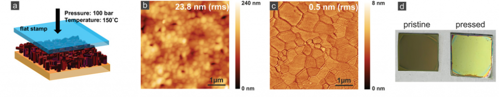
For all active systems we apply a dedicated recrystallization process by thermal imprint (see Figure 1). This way, we aim to achieve larger perovskite crystals, an overall improved crystal quality with less defects, and reduced non-radiative recombination. Larger crystals are also expected to provide improved stability. Depending on the Voc of the sub-cells (~ 1.4-0.5 V) a series connection of 3-8 cells is required to achieve 4 V operating voltage as needed by the TFC. To provide 4 V, the following concepts are considered.
- Connection of cells laterally, e.g. four 2 x 0.5 cm2 cells on 2 x 2 cm2 (for a single cell voltage of 1 V up to 4 V mini-module).
- Monolithic vertical integration of a multi-junction cell (added voltage of the sub-cells).
- A combination of (1)+(2).